The latest “attack” on India’s PLI scheme comes from Bloomberg Andy Mukherjee, someone known to hate India in general and Narendra Modi govt in particular. In his latest piece which is also mirrored here, apart from some specific examples attacking PLI scheme, he also writes
“However, it’s unclear if India has given serious thought to costs and benefits. Take the recently announced joint venture of Taiwan’s Foxconn Technology Group, and the metals company Vedanta Ltd. to set up a $19.4 billion semiconductor factory in Modi’s home state of Gujarat. Last week, the administration announced that it would bear half the cost of such plants, at the top end of its plan of 30% to 50% support. As one opposition politician noted, the Foxconn-Vedanta project would cost the exchequer more than a rural jobs program that sustained 80 million Indians during the pandemic lockdown.”
Comparison of PLI scheme or semiconductor incentive scheme (which is technically not a PLI) to social benefit schemes is totally out of place – in short, the difference between “giving the fish” and “teaching how to fish”. Also, even if one were to compare with the social benefits rolled out by the Modi government during the pandemic, why quote only the figures from “Rural job guarantee scheme”, the free ration scheme is so far costing the government 3.91 lakh crore (close to $50 billion), there were subsidies given for vaccination program. Forget just the pandemic times, even in normal times, many things continue to be subsidized in India and the “burden” is on the exchequer
The need for PLI and semiconductor incentives have been covered by many including me in various articles and so not repeating those, however what is worrying is that suddenly the debate seems to have become more of political in nature. Knowingly or unknowingly, the way Vedanta has handled this so far and continues to handle it seems to have contributed somewhat to it
Fundamentally, my issue with Vedanta has been the lack of transparency and clarity. If they had chosen to simply explain that as “As of now it is between us and the government (MEITY), once it is all final and approved, we will tell you the details”, then perhaps it would been okay to some degree, instead, the path chosen seems to have been one of hype and confusion. I cannot vouch whether this is coming from Vedanta itself or the way media has reported, but here are some examples:
- Based on some quotes from https://www.cnbctv18.com/business/companies/vedanta-foxconn-semiconductor-plant-gujarat-anil-agarwal-independent-agency-selects-location-14722131.htm a report from 14 Sep 2022

“We will not be manufacturing laptops, mobile phones, etc., but we are going to create a cluster to encourage manufacturers,” . What exactly does that mean ? “create a cluster” ? cluster of what ?
2. In the same report, lets take another section
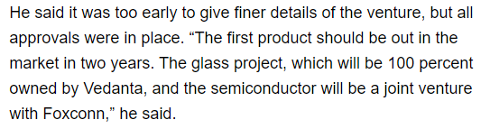
a) What does he mean by “all approvals were in place” when MEITY has not yet approved the incentives due from the Center even as of today (29Sep2022) much less on the day of the report ?
b) “First” product will be out in two years – which product is he talking about ? If it is semiconductor chips, a 28nm fab in India will take 1.5-2 years to construct the factory itself, then equip it, qualify it.. A comparable project is TSMC-Sony-Denso “JASM” fab in Japan. As per this report, construction started in April 2022 and the fab is expected to be operational by Dec 2024 – that is 2 years and 9 months. Sellable chips may come out only 3 years after construction start.. and this is for a project involving the worlds largest foundry TSMC with years of experience whose 28nm technology has been running in high volume production for many years now and it will be a “copy and paste” to Japan
Vedanta’s partner Foxconn on the other hand so far is not known to have any experience in any 300mm wafer fab (which includes 28nm). In fact this is a point where Vedanta has lacked transparency and was even asked by MEITY to provide details. On the one hand, to say that “Its Foxconn’s responsibility to get the tech” as though it is none of Vedanta’s botheration and on the other hand to make sweeping statements like “product in two years” does not augur well at all
3) Let me take another report – this time a full interview published on 08Aug2022 at https://timesofindia.indiatimes.com/city/bengaluru/chip-plant-will-create-another-silicon-valley/articleshow/93382603.cms

First of all, why are you mixing politics and elections into this ? Secondly, that statement about 45nm in August and back to 28nm in September – are you even clear on what you want to do ? And finally, anyone with even some bit of semiconductor knowledge will laugh at your statement in 2022 that “28nm is still in innovation stage”. Making fun is not the intention here, when you are expecting billions of dollars from Central and state governments in subsidies, isn’t there a minimum level of “responsible statements” that one expects ?
4) Back to the 14Sep cnbctv18 report
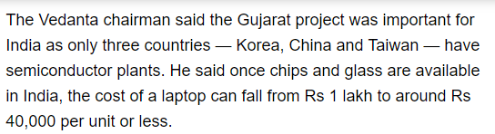
If Anil Agarwal indeed said that, who exactly is he trying to fool ? There are semiconductor fabs in US, multiple countries in Europe like Germany, Italy, France, Israel, in multiple other countries in Asia like Singapore, Malaysia. Now, which Rs 1 lakh laptop currently sold in India (or in in the future) will have key chips (CPU/GPU etc) made using 28nm or 45nm that Vedanta’s fabs will reduce its cost by 60% or more ? Moreover, Do you even understand that the kind of fab you seem to have proposed is foundry model where you contract manufacture your chips for a different company that owns and sells them ?
By the way, it is in the same report/interview that you have said “We will not be manufacturing laptops, mobile phones, etc., but we are going to create a cluster to encourage manufacturers,”
Even if you meant that as a generic statement (“if there were fabs in India for advanced node chips AND Indian companies owning the IP and chip, the cost would have fallen”), there is no real basis for the kind of numbers he has thrown around- the onus is on him to explain how he arrived at those.
5) There has been an overemphasis of “Avanstrate” (we own the glass) as though the glass substrate is the only thing needed for displays. “Glass substrate” is only one part of the puzzle, much more happens on top of it – see https://icea.org.in/blog/wp-content/uploads/2021/05/Displays-Report_20.05.21.pdf . And how much is Avanstrate’s market share ? As per a 2018 report, 2.4%

Now, Foxconn does have a subsidiary – Innolux – experienced in display fabs. However, indications are that Innolux gets the substrate glass from Corning. Interestingly, Vedanta hardly mentions about Innolux in its press releases, but in the semicon conference at Bengaluru in end-April, in the session on display fabs alloted to Vedanta, it was someone from Innolux who explained technical aspects ! Assuming Vedanta may be getting technology from Innolux, whose glass will they use ?
6) Finally, the exact investment details have been very vague. There are different statements at different times – just search in the media and you will know what I mean. Sometimes its 2.04 lakh crore, the latest is 1.54 lakh crore, out of which some media has reported that 94K crore is for display fabs (but as per MEITY data released on 19 Feb 2020, from Vedanta and ELEST together, it got investment proposals worth $6.7 b only which is like 57K crore and Vedanta’s application may be for something like 30K crore only.. and the applications have been closed since 15Feb2022) and 60K crore for semiconductor fab and packaging unit. As per Vedanta’s 13Sep2022 press release

Now, what is that $2 billion “initial investment” all about ? For sure you cannot achieve anything close to a 28nm fab or the required capacity (40000 wafers per month) with $2b. I am not sure even if a display fab can be achieved by then. So then are you talking about start with packaging only ?
So much confusion, at least for the reader. One may say, such confusion and hype are part of how things happen in India – but then in a situation where you are expecting ten-thousands or even lakhs of crore from govt as subsidies, such lack of clarity can only hurt the cause, including other genuine applicants and India’s much needed and already late by decades efforts are building commercial fabs
The government- MEITY, its Ministers and even the Prime Minsiter- too has to ensure that the whole process comes across as transparent to the degree possible, fair (without bias) and based on technological considerations and not based on political or “playing to the gallery” considerations.
